
P-N Junction Diode
P-N Junction Diode: Overview
This topic covers concepts such as p-n junction, potential barrier at the junction diode, forward biasing of junction diode, reverse biasing of junction diode, and characteristic curve of junction diode.
Important Questions on P-N Junction Diode
Semiconductor devices require _____ voltage operation as compared to the vacuum tubes.
The semiconductor device has a _____ size, so the circuits involving devices are very compact.
Semiconductor devices have no filaments hence there is no power needed to heat them to cause the emission of the electrons.
What are the advantages of semiconductor devices?
What is reverse break down of diode?
In a P-N junction, current can go from N side to P side but not from P side to N side.
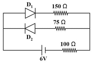
The circuit shown below contains two ideal diodes, each with a forward resistance of If the battery voltage is the current through the resistance (in amperes) is:
Mention some advantages of semiconductor devices.
In reverse bias of a p-n junction diode, the reverse current is very small and is voltage independent upto certain reverse bias voltage, known as
Define breakdown voltage of a diode in reverse bias.
What do you mean by reverse breakdown of diode in reverse bias?
In P type semiconductor pentavalent impurities are used for doping while in N type semiconductor trivalent impurities are used for doping.
The potential in the depletion layer is due to
In a P-N junction, current can go from N side to P side but not from P side to N side.
Explain the working of forward biased and reverse biased p-n junction diode. Draw the characteristic of p-n junction diode.
Explain the formation of potential barrier in a p-n junction.


